A new print-in-place technique for electronics is gentle enough to work on delicate surfaces including paper and human skin, researchers report.
The advance could enable technologies such as high-adhesion, embedded electronic tattoos, and bandages tricked out with patient-specific biosensors.
“When people hear the term ‘printed electronics,’ the expectation is that a person loads a substrate and the designs for an electronic circuit into a printer and, some reasonable time later, removes a fully functional electronic circuit,” says Aaron Franklin, associate professor of electrical and computer engineering at Duke University.
“Over the years there have been a slew of research papers promising these kinds of ‘fully printed electronics,’ but the reality is that the process actually involves taking the sample out multiple times to bake it, wash it, or spin-coat materials onto it,” Franklin says. “Ours is the first where the reality matches the public perception.”
The researchers describe the techniques in two papers, one in Nanoscale and one in ACS Nano.
The origin of electronic tattoos
John A. Rogers, now a professor of materials science and engineering at Northwestern University, first developed the concept of so-called electronic tattoos in the late 2000s at the University of Illinois. Rather than a true tattoo that is injected permanently into the skin, Rogers’s electronic tattoos are thin, flexible patches of rubber that contain equally flexible electrical components.
The thin film sticks to skin much like a temporary tattoo, and early versions of the flexible electronics contained heart and brain activity monitors and muscle stimulators. While these types of devices are on their way to commercialization and large-scale manufacturing, they’re not well-suited in some arenas, such as when direct modification of a surface by adding custom electronics is necessary.
“For direct or additive printing to ever really be useful, you’re going to need to be able to print the entirety of whatever you’re printing in one step,” says Franklin. “Some of the more exotic applications include intimately connected electronic tattoos that could be used for biological tagging or unique detection mechanisms, rapid prototyping for on-the-fly custom electronics, and paper-based diagnostics that could be integrated readily into customized bandages.”
The first paper describes how Franklin’s lab and the laboratory of Benjamin Wiley, professor of chemistry, developed a novel ink containing silver nanowires that can print onto any substrate at low temperatures with an aerosol printer. It yields a thin film that maintains its conductivity without any further processing. After printing, the ink dries in less than two minutes and retains its high electrical performance even after enduring a 50% bending strain more than a thousand times.

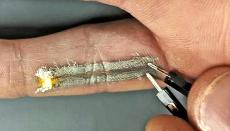
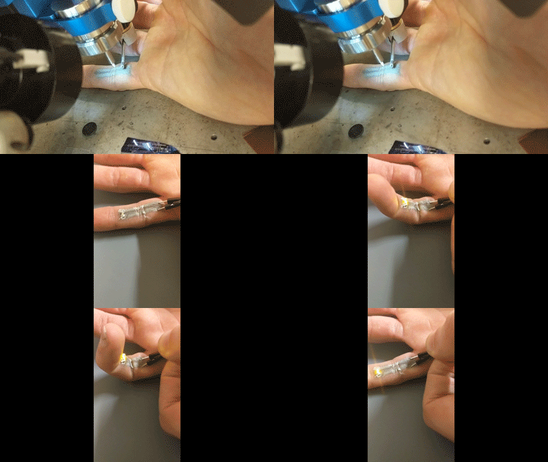
In a video accompanying the first paper, graduate student Nick Williams prints two electronically active leads along the underside of his pinky finger. Toward the end of his finger, he connects the leads to a small LED light. He then applies a voltage to the bottom of the two printed leads, causing the LED to stay lit even as he bends and moves the finger.
In the second paper, Franklin and graduate student Shiheng Lu take the conductive ink a step further and combine it with two other printable components to create functional transistors. The printer first puts down a semiconducting strip of carbon nanotubes. Once it dries, and without removing the plastic or paper substrate from the printer, the printer creates two silver nanowire leads that extend several centimeters from either side. It then prints a non-conducting dielectric layer of a two-dimensional material, hexagonal boron nitride, on top of the original semiconductor strip, followed by a final silver nanowire gate electrode.
A better process for printed electronics
With today’s technologies, at least one of these steps would require the removal of the substrate for additional processing, such as a chemical bath to rinse away unwanted material, a hardening process to ensure layers don’t mix, or an extended bake to remove traces of organic material that can interfere with electric fields.
But Franklin’s print-in-place requires none of these steps and, despite the need for each layer to dry completely to avoid mixing materials, works at the lowest overall processing temperature reported to date.
“Nobody thought the aerosolized ink, especially for boron nitride, would deliver the properties needed to make functional electronics without being baked for at least an hour and a half,” says Franklin. “But not only did we get it to work, we showed that baking it for two hours after printing doesn’t improve its performance. It was as good as it could get just using our fully print-in-place process.”
Franklin doesn’t see his printing method replacing large-scale manufacturing processes for wearable electronics. But he does see a potential value for applications such as rapid prototyping or situations where one size doesn’t fit all.
“Think about creating bespoke bandages that contain electronics like biosensors, where a nurse could just walk over to a work station and punch in what features were needed for a specific patient,” says Franklin. “This is the type of print-on-demand capability that could help drive that.”
Support for the work came from the Department of Defense Congressionally Directed Medical Research Program, the National Institutes of Health, and the National Science Foundation.
Source: Duke University
The post Light-up tattoos use electronics printed right onto skin appeared first on Futurity.
from Futurity https://ift.tt/2pEzL8L
No comments:
Post a Comment